ElectraTech works with the customer to design the circuit board according to their specific requirements and specifications. This may include creating the layout and schematics for the circuit, selecting the appropriate materials and components, and simulating the circuit to ensure that it will function as intended.
Our team of experienced engineers specializes in PCB design and layout using industry-standard software such as Altium Designer. We have the skills and knowledge to design PCBs for a wide range of applications and industries, including telecommunications, consumer electronics, medical devices, and more.
General Design Capabilities
Analog and Mixed-Signal Designs.
High Density and Complex Designs.
High-Speed Digital Designs.
RF Designs.
We take pride in delivering high-quality PCB designs that meet all necessary specifications and requirements. Our rigorous design process includes multiple rounds of review and testing to ensure that the final product is reliable and ready for production.
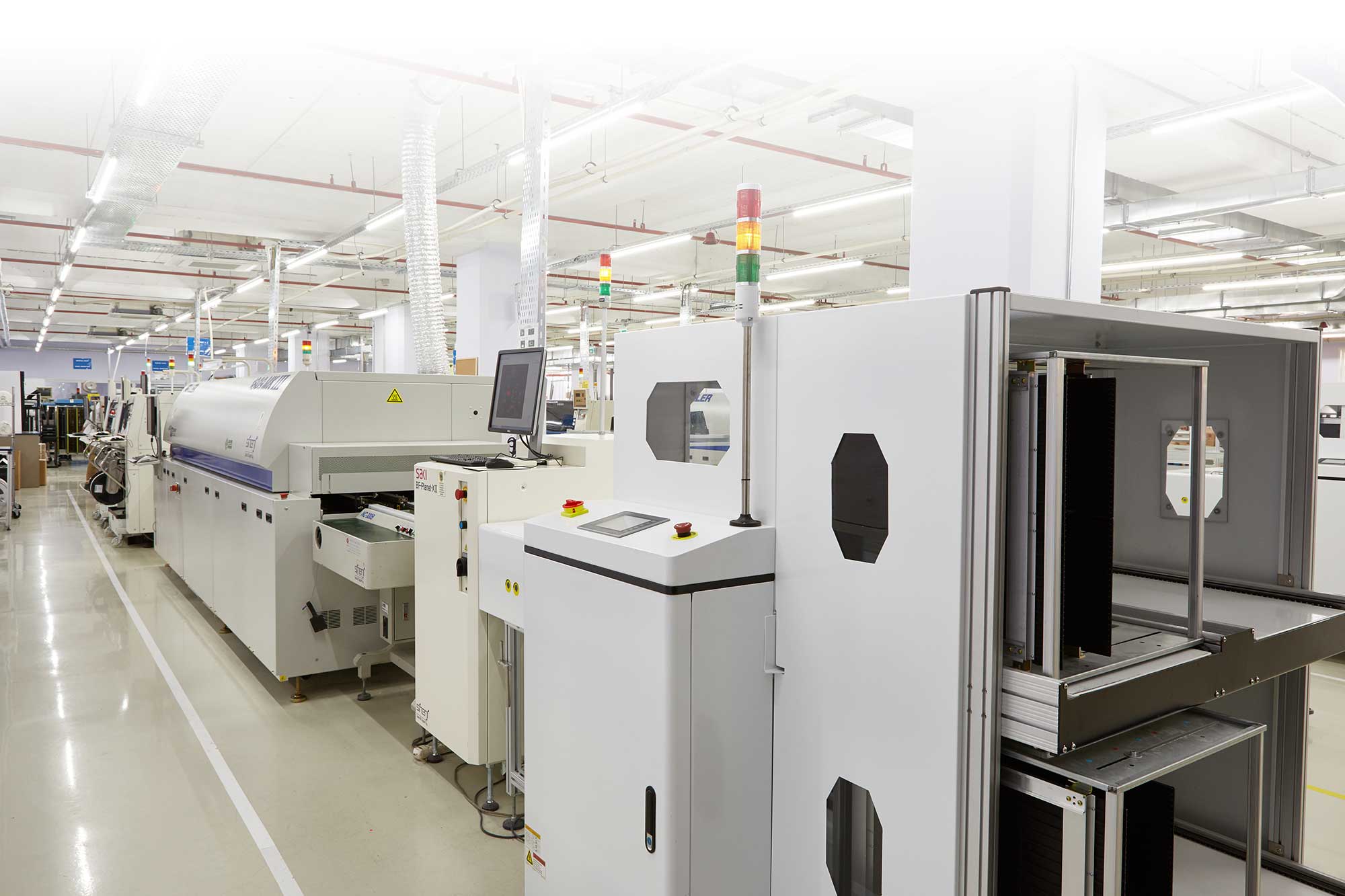
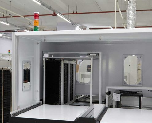
Assembly Lines:
Our Assembly Lines feature with various setups, suitable for different production requirements. The lines consist of below equipments:
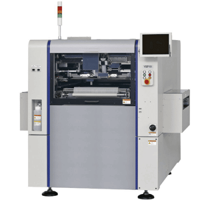
Automatic Stencil Printer
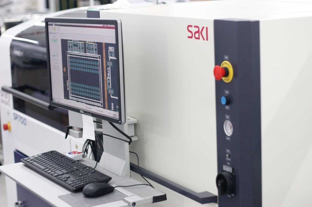
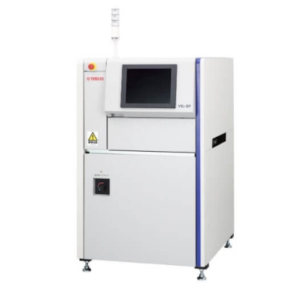
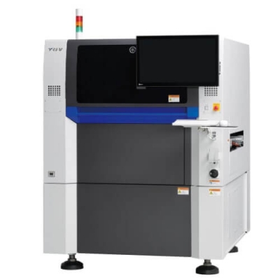
3D SPI (Solder Paste Inspection System)
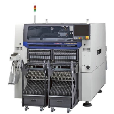
High-speed / medium-speed Pick-and-Place Machine
Multi-Function IC Mounter
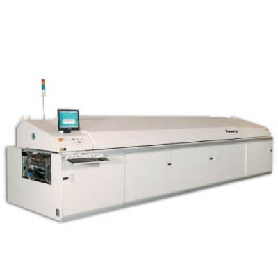
8 Heat-Zone Reflow Machine
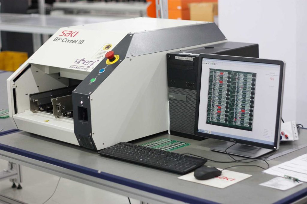
Automatic Optical Inspection System
Solder Paste
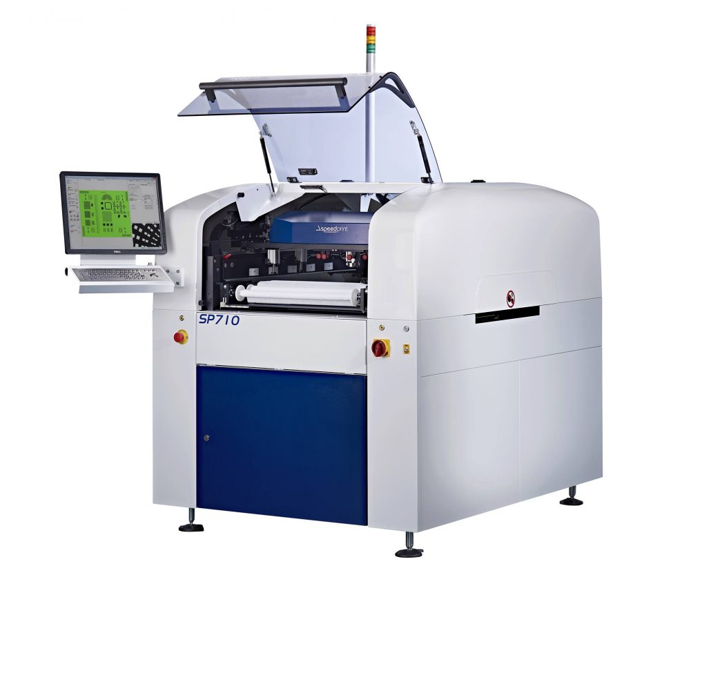
Our fully automatic screen printer machine performs solder spread process using definite stencils specially produced for each printed circuit board.
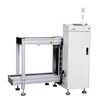
PCB Loader
We have 3 SMD assembly lines which are equipped with PCB loader, magazine loader, NG-OK magazine unloader, completely automatic Screen Printer, SPI, AOI, Pick and Place ve X-ray machines with 9 zone reflow soldering furnaces.
Pick and Place
Using our P&P machines, we can assembly to PCB 360.000 component per hour with definite coordinates, appropriate angle and height.
Solder Paste Inspection
SPI machine is able to fix solder paste defects that provides an opportunity to get rid of defected boards before they will be used in production process. While performing this process, we can examine the solder height with 10 micron precision using 3D feature of SPI machine.
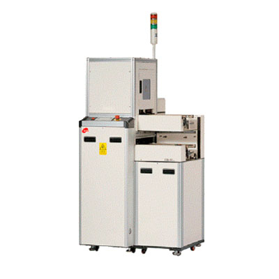
NG/OK Unloader
This machine can buffer the NG and Ok boards from AOI and SPI. The okay board will flow into the next programme and the NG board will flow to the storage magazine of machine. PCB Un-loader The PCB Loader is designed for loading of PCBs. The unit loads your production line automatically by pushing PCB’s out of a magazine onto the conveyor of the down-stream machine. Connect with SMT and AI productions line, safety design ensure not to break any PCB when it is pushed and thus reduce defect rate. PCB Loader The PCB Unloader is designed for unloading of PCBs, an arriving PCB is taken up by the attached conveyor and then pushed into the magazine by a specially designed pusher. The magazine indexes to the next position and is ready for the following unloading cycle.
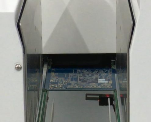
Automated Optical Inspection
With our AOI machines, we are able to perform all the final control operations such as detecting soldering defects, wrong position of the components and detecting any errors in the manufacturing process that assures process quality before the boards are moved to the next manufacturing step.
The PCB Loader is designed for loading of PCBs. The unit loads your production line automatically by pushing PCB's out of a magazine onto the conveyor of the down-stream machine.
Solder paste printer is the latest high-speed screen printer specified for big-size PCBs with machine vision automatic identification, cloud manufacturing, and other technical innovation.
Solder paste inspection is an Automation system that combines the production characteristics of major factories. It has the characteristics of stable performance.
Juki pick and place machines perform high-quality work while ensuring overall precision and accuracy of component placement on PCBs Surface Mount Machines are also called Pick-and-place machines.
The PCB Unloader is designed for unloading of PCBs, an arriving PCB is taken up by the attached conveyor and then pushed into the magazine by a specially designed pusher.
This machine can buffer the NG and Ok boards from AOI and SPI. The okay board will flow into the next program and the NG board will flow to the storage magazine of the machine.
Reflow oven is the most cutting edge technology, specializing in production and sale of a full series of wave soldering equipment. Used for SMT SMA SV PV PCB CBS.
Automatic optical inspection is professional product use to inspect the welding quality and installation status of surface mount device on SMT production line.